
1.4K
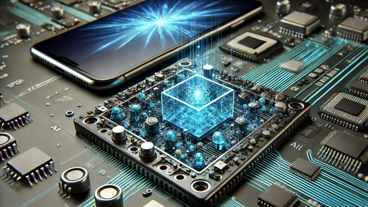
In the accelerating landscape of advanced electronics, nanotechnology has emerged as the cornerstone of innovation, particularly in the domain of semiconductor fabrication. The launch of Apple’s A17 Pro and the newly introduced A18 chip, both leveraging 3-nanometer (nm) process technology, signals a decisive leap in nano-engineered chip architecture. These chips are not merely iterations of prior models but are manifestations of the profound shifts in material science and atomic-scale engineering. This article delves deeply into the nanotechnological principles that underlie these chips, analyzing their design, implications for performance and sustainability, and their broader role in the evolution of computation.
Nanotechnology in Semiconductor Engineering: Principles and Paradigms
At its essence, nanotechnology involves manipulating matter at dimensions typically below 100 nanometers. Within this scope, transistors—the fundamental switching elements in chips—are engineered at near-atomic scales. Shrinking transistor nodes from 4 nm to 3 nm is not a trivial dimensional reduction; it introduces entirely new quantum mechanical behaviors, challenges in electrostatics, and demands for material innovation in gate dielectrics and interconnects.
The 3nm FinFET architecture, utilized in the TSMC N3B and N3E fabrication processes, empowers chipmakers to dramatically increase transistor density, reduce leakage currents, and improve switching speed. For Apple, this has translated into 19 billion transistors on the A17 Pro and an even denser configuration in the A18, paving the way for transformative computational capabilities in mobile devices.
The 3nm Advantage: Scientific Foundations and Engineering Gains
1. Transistor Density and Performance Scaling
The A18 and A17 Pro benefit from ultradense transistor integration, allowing Apple to enhance processing throughput and support complex, parallelized computations. This is critical for:
Real-time AI inference
Hardware-accelerated ray tracing for advanced graphics rendering
Neural network engines for computational photography and AR applications
Each transistor switch operates faster and more efficiently, a direct benefit of shorter gate lengths and improved channel control in the 3nm regime.
2. Energy Efficiency through Gate-All-Around (GAA) Prospects
While Apple currently employs FinFETs, the shift to Gate-All-Around FETs (GAAFETs) in upcoming nodes (e.g., 2nm) is already on the horizon. The 3nm process lays the groundwork by refining power gating techniques, dynamic voltage scaling, and active power management, all vital in reducing battery consumption and thermal output.
3. Thermal Management and Materials Innovation
At nanoscale dimensions, thermal conduction becomes a limiting factor. Apple’s chip design incorporates advanced heat spreaders, low-k dielectrics, and optimized substrate materials to maintain thermal stability. This is critical for maintaining performance consistency under sustained workloads.
The A18 and A17 Pro: Case Studies in Applied Nanotechnology
The A18 chip, presumed to be fabricated using TSMC’s second-generation 3nm N3E process, builds upon the achievements of the A17 Pro with even finer transistor uniformity and improved yields.
Key Innovations Enabled by Nanotechnology:
Increased neural engine performance for low-latency AI processing
Enhanced GPU architecture supporting real-time 3D rendering
Superior image signal processing using custom ML models on silicon
Integrated secure enclave enhancements at the hardware level
Together, these advances support Apple’s broader integration of on-device intelligence, augmented reality, and computational imaging, underscoring the transformative power of nanoscale design.
Implications Beyond Mobile: The Broader Reach of 3nm Nanotech
1. Artificial Intelligence and Machine Learning
The computational intensity of AI workloads necessitates ultra-efficient processing units. Apple’s A18 architecture exemplifies how nanotechnology facilitates tensor acceleration, enabling larger transformer models and on-device learning, paving the way for private, fast, and adaptive AI systems.
2. Biotechnology and Medical Devices
The principles used in 3nm chip design are being mirrored in bio-integrated nanosensors, implantable diagnostics, and lab-on-chip systems. The miniaturization and power efficiency demonstrated by chips like the A18 suggest a convergent future where health monitoring and mobile computing are seamlessly intertwined.
3. Sustainability and Green Computing
Nanotechnology’s contribution to energy-efficient semiconductors is indispensable in the quest for sustainable electronics. By reducing power consumption while increasing processing capabilities, chips like A18 align with global goals for carbon neutrality, e-waste reduction, and resource-efficient manufacturing.
Future Directions: Scaling Beyond 3nm
The current achievements at the 3nm node are remarkable, but semiconductor roadmaps already anticipate sub-3nm architectures. Emerging research focuses on:
2nm and 1.4nm GAAFETs
Monolithic 3D chip stacking
2D materials like graphene and molybdenum disulfide
Photonic interconnects to replace copper wiring bottlenecks
Each of these innovations will require a deeper integration of quantum physics, materials science, and nanoscale metrology to address the limitations of current silicon-based systems.
Conclusion
The Apple A18 and A17 Pro chips stand as tangible evidence of how nanotechnology has become not just a tool, but a scientific imperative in modern computing. By mastering the 3nm process, Apple has demonstrated the unmatched potential of nanoscale engineering to elevate performance, enhance efficiency, and expand the functional possibilities of mobile devices.
In a broader context, these innovations mark a turning point in how computational power is conceived, delivered, and applied—from personal devices to global infrastructures. As the nanotechnological frontier continues to advance, the convergence of miniaturization, intelligence, and sustainability will define the next generation of technological evolution.