
359
Scanning Electron Microscopy (SEM) has emerged as an indispensable tool for high-resolution surface imaging and compositional analysis, reshaping the landscape of scientific discovery and industrial innovation. With its unparalleled resolution and signal detection capabilities, SEM enables visualization of surface topographies and microstructural features at the nanometer scale—capabilities that far exceed the limitations of conventional optical microscopy. Its versatility and adaptability have led to widespread adoption across domains including nanotechnology, materials engineering, life sciences, and semiconductor device fabrication.
Operational Principles of Scanning Electron Microscopy
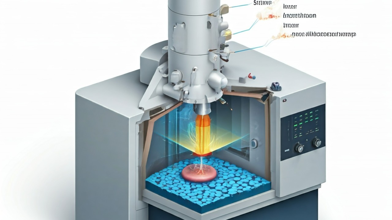
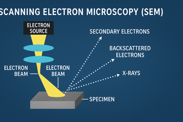
SEM operates on the principle of electron-specimen interaction. A finely focused electron beam is rastered across the surface of a solid sample under vacuum conditions. As the primary electrons penetrate the sample surface, they generate several types of emissions—primarily secondary electrons (SEs), backscattered electrons (BSEs), and characteristic X-rays—each offering distinct insights into the sample’s morphology and composition.
Secondary electrons, originating from surface atoms, are typically used for high-resolution topographic imaging. Backscattered electrons provide atomic number contrast, enabling compositional differentiation. The emitted X-rays, when analyzed via energy-dispersive X-ray spectroscopy (EDS), facilitate qualitative and quantitative elemental analysis. Modern SEM systems can resolve features as small as 1–2 nanometers, making them ideal for applications where nanoscale precision is required.
Advanced SEM Techniques
Cryogenic SEM (Cryo-SEM)
Cryo-SEM is particularly advantageous in the study of biological and polymeric materials that are sensitive to dehydration and conventional preparation procedures. By cryogenically freezing the sample, structural integrity is preserved, enabling high-fidelity imaging of hydrated biological tissues, liposomes, hydrogels, and other soft matter systems without structural collapse or artefactual distortion.
Low-Temperature SEM (LTSEM)
LTSEM facilitates the observation of biological samples in a near-native hydrated state. This technique maintains water content, avoids fixation-induced artefacts, and is critical in the analysis of living tissues, cellular structures, and microbial morphologies under physiologically relevant conditions.
SEM-EDS (Energy-Dispersive X-ray Spectroscopy)
The integration of EDS with SEM systems allows real-time elemental mapping and point-specific chemical analysis. This dual-capability is vital in applications such as failure analysis, alloy characterization, mineral identification, and thin-film composition verification.
Interdisciplinary Applications of SEM
Biological Sciences
SEM has redefined the visualization of biological specimens by allowing high-resolution surface imaging of cellular and subcellular architectures. Applications range from studying morphological adaptations in plant and animal cells to microbial colonization patterns. LTSEM and Cryo-SEM provide critical insights into tissue interfaces, biofilms, and ultrastructural dynamics of organelles with minimal sample perturbation.
Nanotechnology and Nanomaterials
SEM is central to the characterization of nanomaterials, including carbon nanotubes, quantum dots, graphene sheets, nanowires, and nanocomposites. These materials often exhibit size-dependent properties, and precise morphological evaluation is essential for correlating structural features with electrical, mechanical, and thermal performance. In nanofabrication, SEM aids in verifying the fidelity of pattern transfer, assessing etch profiles, and optimizing feature alignment during lithographic processes.
Materials Science and Engineering
In materials research, SEM serves as a diagnostic platform for analyzing phase boundaries, grain structures, dislocation networks, and fracture surfaces in metallic, ceramic, polymeric, and hybrid materials. This information informs material selection, processing optimization, and failure mitigation strategies. SEM is also pivotal in corrosion studies, diffusion behavior assessment, and interface characterization in composite systems.
Semiconductor Industry
The semiconductor industry extensively utilizes SEM for inline defect inspection, process control, and failure analysis. Charge Collection SEM (CC-SEM), a specialized mode, enables the mapping of electrical activity across semiconductor junctions. It provides crucial information on charge carrier distribution, p-n junction defects, and dielectric breakdown, directly impacting device yield and performance. SEM also supports critical dimension (CD) measurement in advanced node lithography processes.
Conclusion
The transformative capabilities of Scanning Electron Microscopy in modern science have made it a foundational imaging and analytical tool across numerous disciplines. Its ability to deliver nanometer-scale resolution, combined with integrated compositional analysis, allows researchers and engineers to probe the intricate structures and properties of matter with remarkable clarity and precision.
As SEM technology evolves—through innovations such as environmental SEM (ESEM), variable pressure systems, and correlative microscopy—it continues to expand the frontiers of high-resolution characterization. Whether in academic research, industrial quality assurance, or applied materials development, SEM remains a critical enabler of scientific progress in the 21st century.
You Might Be Interested In
- The Complete Guide to Nanotechnology and Nanoscience Education: Top Colleges, Costs, Careers, and Specializations
- The Future of Nanotechnology: 10 Emerging Trends Shaping Innovation in 2025 and Beyond
- MIT Physicists Capture First Real-Space Images of Free-Interacting Atoms
- Quantum Dot Nanotechnology: Revolutionizing Targeted Drug Delivery in Oncology