
711
A PhD in nanotechnology is more than an academic degree — it’s a gateway to contributing to cutting-edge innovation in medicine, energy, materials, and electronics. While the idea of pursuing such a degree abroad may feel overwhelming, the journey becomes clearer and more achievable with strategic planning.
In this article, we’ll walk through how to prepare, apply, and thrive in an international nanotechnology PhD program, plus we’ll explore real costs, funding sources, common mistakes, and a mind map to keep your path structured.
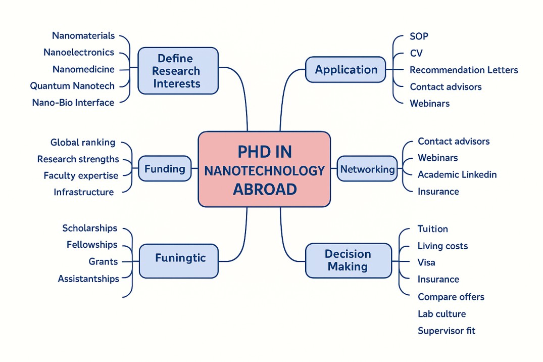
Mind Map: Your PhD in Nanotechnology Abroad Roadmap
(Visual representation – can be turned into an infographic for your site)
Main Goal → PhD in Nanotechnology Abroad
Branches:
-
Define Research Interests → Nanomaterials, Nanoelectronics, Nanomedicine, Quantum Nanotech, Nano-Bio Interfaces
-
University Search → Top global nanotech hubs (IISc-linked collaborations, MIT, ETH Zurich, NUS, Cambridge)
-
Funding & Scholarships → DAAD, Erasmus Mundus, Marie Skłodowska-Curie, Fulbright, Commonwealth, University-specific fellowships
-
Application Preparation → SOP, CV, Recommendation Letters, Test Scores (GRE, TOEFL/IELTS)
-
Networking → Contact advisors, attend webinars, academic LinkedIn outreach
-
Financial Planning → Tuition, living costs, visa, insurance
-
Decision-Making → Compare offers, research lab culture, supervisor fit
1. Define Your Research Interests
Nanotechnology is vast. Be precise about your focus — it helps target the right universities and advisors.
Popular PhD subfields include:
-
Nanomaterials for energy storage & conversion
-
Nanoelectronics & quantum devices
-
Nanomedicine & targeted drug delivery
-
NEMS/MEMS engineering
-
Environmental nanotechnology
Pro Tip: Review recent publications from leading journals (Nature Nanotechnology, ACS Nano) to spot trending research topics.
2. Research Global Universities & Labs
Shortlist institutions based on research alignment and global ranking in nanoscience.
Examples of Top Global Options:
-
USA: MIT, Stanford, UC Berkeley, Rice University
-
Europe: ETH Zurich (Switzerland), University of Cambridge (UK), Delft University of Technology (Netherlands)
-
Asia-Pacific: National University of Singapore (NUS), University of Tokyo (Japan)
-
Australia: University of Queensland, Monash University
Selection Criteria:
-
Faculty expertise & publications
-
Research infrastructure (clean rooms, electron microscopes, nanofabrication centres)
-
Collaboration with industry or government
3. Build a Strong Academic Profile
-
Maintain a GPA above 3.5/4.0 or equivalent (>75% in Indian grading)
-
Undertake relevant projects or internships in nanotechnology labs
-
Publish papers or present at conferences to strengthen your research credibility
4. Prepare Application Materials
Statement of Purpose (SOP)
Explain:
-
Why nanotechnology fascinates you
-
Your research experience & skills
-
How the program aligns with your goals
-
Why that specific university is the right fit
Recommendation Letters
Get 3 strong academic references — ideally from supervisors who know your research capabilities well.
Tests
-
GRE (if required): Target >320
-
TOEFL iBT: >95 or IELTS: 7.0+
5. Funding Options & Scholarships
Fully Funded Schemes:
-
Marie Skłodowska-Curie Actions (EU) – Stipend €3,500–€4,000/month
-
DAAD Research Grants (Germany) – €1,200/month + travel & insurance
-
Erasmus Mundus Joint Doctorates – Full tuition + €1,500/month
-
Fulbright (USA) – Covers tuition & living costs
-
Commonwealth Scholarships (UK) – Covers tuition, airfare, stipend (~£1,300/month)
University Fellowships:
Most top universities offer fully-funded PhDs where tuition is waived and students receive a stipend.
6. Estimated Cost of Study Abroad (If Self-Funded)
| Region | Annual Tuition | Living Costs | Total per Year |
|---|---|---|---|
| USA | $25,000–$50,000 | $15,000–$20,000 | $40,000–$70,000 (₹33–58 lakh) |
| UK | £15,000–£30,000 | £12,000–£18,000 | £27,000–£48,000 (₹28–50 lakh) |
| Europe (Germany, France) | €0–€5,000 | €10,000–€15,000 | €10,000–€20,000 (₹9–18 lakh) |
| Australia | AUD 30,000–40,000 | AUD 20,000–25,000 | AUD 50,000–65,000 (₹27–35 lakh) |
7. Pros & Cons of Pursuing a PhD Abroad
✅ Advantages:
-
Access to cutting-edge research facilities
-
Higher stipends and funding availability
-
Global networking & career opportunities
-
Exposure to interdisciplinary research
⚠️ Challenges:
-
Competitive admission process
-
Cultural & academic adjustment
-
Time commitment (3–6 years)
-
Possible relocation stress & visa hurdles
8. Key Action Checklist
✔ Define specialization within nanotechnology
✔ Shortlist 8–10 universities globally
✔ Prepare SOP, CV, recommendations, test scores
✔ Research & apply for scholarships early
✔ Contact potential supervisors
✔ Compare offers based on funding, research fit, and location
Conclusion
A PhD in nanotechnology abroad is a high-investment, high-reward journey. With the right planning — from defining your research niche to securing funding — you can turn this dream into reality. Remember, success comes from clarity, preparation, and persistence.
Whether you aim to design next-gen medical nanorobots, develop sustainable nanomaterials, or pioneer quantum devices, your journey starts with the first step — preparing today.
Table of Contents
previous post