
1
Key Highlights
- IBM introduces the world’s first sub-1 nanometer (0.7 nm / 7 angstrom) chip technology.
- Built using the revolutionary 3D Nanostack transistor architecture.
- Packs nearly 100 billion transistors on a fingernail-sized chip.
- Delivers up to 50% higher performance or 70% greater energy efficiency than IBM’s 2 nm chips.
- Demonstrates 40% SRAM scaling for AI and high-performance computing.
- Commercial adoption is expected within the next five years.
IBM Achieves a Major Semiconductor Breakthrough
IBM has announced a significant milestone in semiconductor research by introducing the world’s first sub-1 nanometer (0.7 nm / 7 angstrom) chip technology. The breakthrough represents a major advancement beyond traditional transistor scaling and demonstrates that semiconductor innovation can continue even as device dimensions approach the size of individual atoms.
The new chip integrates nearly 100 billion transistors onto a chip approximately the size of a fingernail—almost twice the transistor density of IBM’s 2 nm chip introduced in 2021.
According to IBM, the technology is projected to provide:
- Up to 50% higher performance, or
- Up to 70% greater energy efficiency
compared with its previous 2 nm technology, making it highly suitable for artificial intelligence (AI), cloud computing, data centers, and next-generation electronic devices.
What is IBM’s Nanostack Architecture?
The key innovation behind this breakthrough is IBM’s Nanostack architecture, the industry’s first known three-dimensional nanosheet-based transistor design.
Unlike conventional transistor layouts that place devices side by side, Nanostack vertically stacks and staggers transistors using 3D sequential integration. This approach significantly increases transistor density while allowing different material combinations to be optimized within each stacked layer for improved performance and power efficiency.
IBM researchers successfully validated the technology through:
- Ultra-thin dielectric bonding
- CMOS integration
- Dual-channel engineering
- Functional CMOS inverter operation
These demonstrations confirm that the architecture can support real semiconductor computing.
Designed for the AI Era
Modern AI applications require enormous computing power and memory bandwidth.
To address these challenges, IBM researchers also demonstrated:
- 40% SRAM scaling
- Improved memory density
- Better support for high-bandwidth AI workloads
These improvements make the technology well suited for future AI accelerators, cloud infrastructure, and high-performance computing systems.
Roadmap Beyond the 1 Nanometer Era
IBM states that its new technology extends semiconductor scaling below the 1 nm node, opening the door to the angstrom era of chip manufacturing.
The company believes the Nanostack architecture will support at least another decade of semiconductor scaling, helping overcome many of the physical limitations facing conventional transistor designs.
Advanced Manufacturing Partnerships
IBM continues to collaborate with several leading semiconductor equipment manufacturers, including:
- ASML
- Lam Research
- Tokyo Electron (TEL)
- SCREEN Semiconductor Solutions
These partnerships focus on developing High Numerical Aperture Extreme Ultraviolet (High-NA EUV) lithography, a critical technology for manufacturing future generations of advanced semiconductor devices.
Commercial Outlook
IBM expects the earliest commercial adoption of its sub-1 nanometer Nanostack technology within the next five years.
The company also recently announced plans to establish Anderon, the world’s first pure-play quantum foundry, further strengthening its long-term strategy in semiconductor manufacturing and quantum computing.
Conclusion
IBM’s sub-1 nanometer chip represents one of the most significant semiconductor breakthroughs in recent years. By introducing the revolutionary 3D Nanostack architecture, IBM has demonstrated that transistor scaling can continue beyond today’s limits while delivering substantial improvements in performance and energy efficiency.
If successfully commercialized, this technology could play a major role in powering the next generation of AI systems, cloud infrastructure, data centers, smartphones, and future computing platforms.
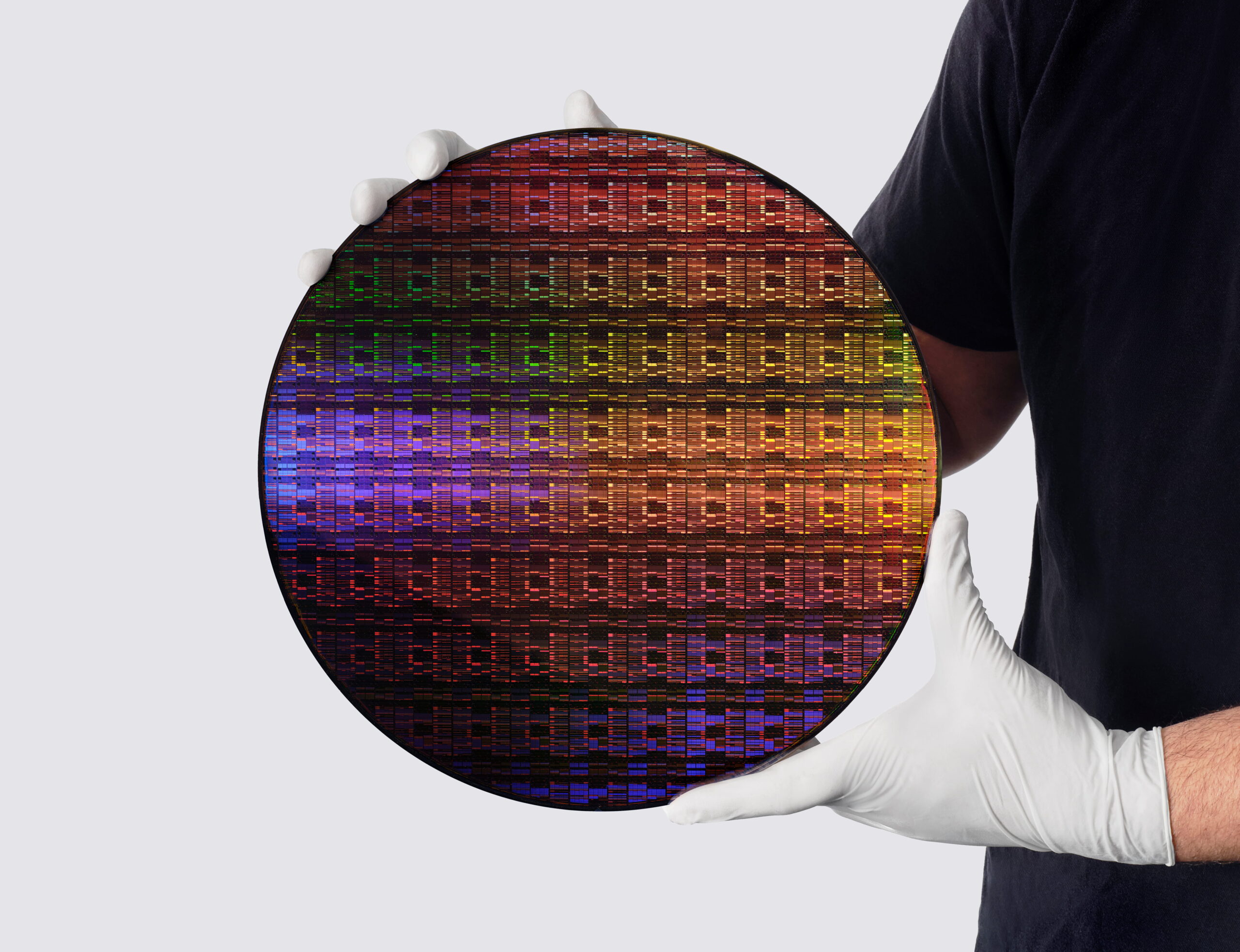
Image Credit: IBM Research
Table of Contents