
11
A doctoral degree or advanced research background in nanotechnology rarely leads to a business card that reads “Nanotechnologist.” In modern industrial settings, nanoscale expertise almost never exists as an isolated title. Instead, it is embedded within critical engineering and R&D functions: Materials Scientist, Semiconductor Process Engineer, Formulation Scientist, Battery Development Engineer, and Metrology Specialist.
For early-career researchers, PhD graduates, and postdoctoral fellows stepping into the private sector, understanding this structural distinction is often the difference between a stalled job search and a high-impact technical career. Nanotechnology has matured beyond its origins as an exploratory scientific discipline into an enabling technological platform. To the organizations driving industrial innovation, the critical asset is not the label of the material, but the operational ability to control physical behavior at the atomic and molecular scale.
The Industrial Reality: A Platform, Not an Industry
Data from the National Nanotechnology Coordination Office (NNCO) frames nanotechnology across several broad operational vectors: advanced computing, biotechnology, energy storage, transportation, and civil infrastructure. Rather than operating as an independent industrial vertical, nanotechnology behaves like software or advanced metallurgy it serves as a foundational platform that enhances adjacent sectors.
The connection between academic nanotechnology research and industrial careers becomes clearer when research expertise is viewed in terms of the functions it enables. Experience in nanoparticle synthesis can translate into roles such as Formulation Chemist or CMC Scientist, while expertise in thin-film deposition and lithography can support careers as a Semiconductor Integration Engineer. Researchers skilled in TEM, SEM, AFM, and XPS analysis can move into Failure Analysis or Metrology Engineering, where advanced characterization is used to evaluate materials and device performance. Expertise in surface functionalization can lead to roles such as Coatings Engineer or Biosensor Scientist, particularly in applications involving engineered interfaces. Similarly, experience with electrochemical nanomaterials can translate into positions such as Battery Materials Scientist or Cell Engineer, where nanoscale materials are developed and optimized for energy-storage applications.
This dynamic explains why scanning job boards exclusively for the keyword “nanotechnology” artificially restricts opportunity. Commercial enterprises recruit for the engineering bottlenecks they need to eliminate, not the academic degree program of the applicant.
Data from the U.S. Bureau of Labor Statistics (BLS) indicates sustained demand for chemists and materials scientists, projecting employment growth of approximately 7% to 8%, depending on the occupational category. Capturing these opportunities requires recognizing where nanoscale phenomena drive commercial value.
- Semiconductors, Nanoelectronics, and Quantum Technologies
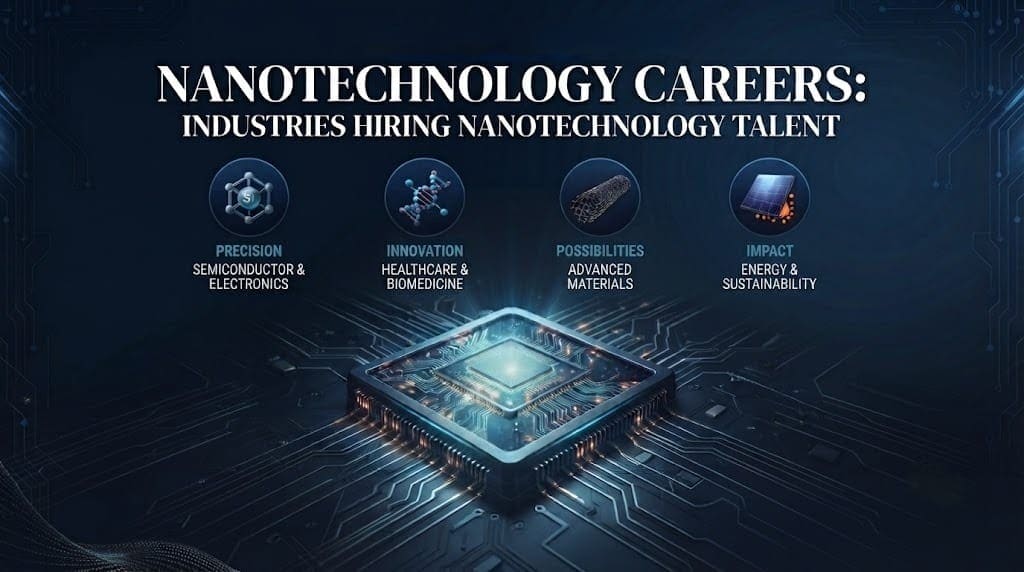
Semiconductor fabrication is applied nanotechnology operating at massive commercial scale. As fabrication facilities advance toward increasingly small process dimensions, controlling thin-film interfaces, gate dielectrics, nanoscale structures, and sub-surface defects become critical to device performance and manufacturing yield.
Technical bodies such as the National Institute of Standards and Technology (NIST) prioritize advanced measurement science, materials characterization, and nanoscale metrology as important components of modern microelectronics development. Nanoscale research directly intersects with atomic layer deposition and chemical vapor deposition for controlled thin-film growth, advanced metrology using techniques such as atomic force microscopy and transmission electron microscopy, and the development of quantum and photonic devices based on structures including quantum dots, plasmonic materials, and other nanoscale architectures.
In this sector, the competitive advantage belongs to candidates who can connect physical characterization with fabrication metrics such as defect density, dimensional control, device performance, reliability, and manufacturing yield.
These skills translate into several closely related industrial functions. Researchers experienced in thin-film deposition, lithography and process optimization may move into semiconductor process integration and thin-film engineering, while expertise in nanoscale characterization can lead toward metrology and failure-analysis functions. Work involving quantum or photonic structures can similarly connect with device integration and advanced materials development. The common industrial requirement is the ability to control, characterize and troubleshoot materials and structures at increasingly small length scales.
- Nanomedicine, Biopharma, and Clinical Diagnostics
Within pharmaceutical development and medical technologies, nanoscale engineering operates at the interface of formulation science, biochemistry, materials science, and regulatory compliance. Nanomaterials can function as delivery systems, formulation components, or signal-transduction elements in diagnostic technologies.
The U.S. Food and Drug Administration (FDA) provides guidance on drug products containing nanomaterials and emphasizes the importance of understanding their physicochemical characteristics, manufacturing processes, and critical quality attributes. For researchers transitioning from academic synthesis laboratories, this shifts the focus from simply producing a novel nanoscale carrier to demonstrating reproducibility, stability, physicochemical integrity, and biological performance.
Relevant considerations can include hydrodynamic particle diameter, particle-size distribution, morphology, aggregation state, surface characteristics, zeta potential, and chemical and physical stability. Nanotechnology-enabled drug-delivery platforms can include liposomes, lipid nanoparticles, polymeric nanoparticles, nanocrystals, and other nanoscale systems designed to influence drug distribution, stability, or release. The same scientific principles extend into biosensing and diagnostics. Gold nanoparticles, quantum dots, carbon-based nanomaterials, plasmonic structures, and nanostructured electrodes can be engineered to generate optical, electrical, or electrochemical signals in analytical systems.
In industry, these capabilities are distributed across formulation, drug-delivery, biointerface and analytical-development functions. Researchers working with nanoparticles, liposomes or lipid nanoparticles may transition into formulation development or CMC-oriented roles, where particle size, morphology, surface properties, stability and reproducibility become important development parameters. Expertise in engineered biological interfaces can also support nanomedicine and biosensor development, particularly where nanoscale materials are used to improve molecular recognition, signal generation or delivery. The job titles vary across pharmaceutical, biotechnology and diagnostics companies, but the underlying requirement is the same: converting nanoscale material behavior into reproducible and measurable biological performance.
- Energy Storage and Advanced Functional Materials
Clean-energy technologies rely on interfacial materials engineering, where energy storage systems depend heavily on nanoscale architectures, solid-electrolyte interphases, and coatings to ensure ion transport, electronic conductivity, and structural integrity against degradation. Beyond batteries, nanoscale engineering enhances electrocatalysis, fuel cells, and thermoelectric devices by optimizing active surface sites and interfacial behavior. Similarly, advanced materials like graphene, carbon nanotubes, and polymer nanocomposites are engineered to modify mechanical, electrical, thermal, and optical properties, underpinning strategic European initiatives across energy, electronics, mobility, and industrial manufacturing.
The nanoscale expertise is increasingly relevant to battery and advanced-materials development. Researchers who understand electrochemical interfaces, electrode architecture and nanoscale transport can contribute to battery-materials and cell-development programs, while experience with surface modification and functional coatings can support electrode, protective-coating and interface engineering. Nanocomposite research involving graphene, carbon nanotubes or other engineered fillers can similarly translate into composite-materials development and performance optimization. In these environments, employers typically value the ability to connect nanoscale structure and surface chemistry with measurable properties such as conductivity, stability, mechanical performance, cycle life and electrochemical efficiency.
- Environmental Remediation, Agri-Tech, and Consumer Products
Nanoscale properties such as high specific surface area, tunable surface chemistry, and size-dependent physical behaviour provide opportunities in environmental and industrial remediation. Nanostructured membranes, adsorbents, photocatalysts, and sensing materials can be investigated for applications involving water purification, contaminant detection, separation, and remediation.
Water-treatment research can involve engineered membranes and functional surfaces designed to improve selective transport, adsorption, or degradation of contaminants. In environmental nanotechnology, however, technological performance must be evaluated alongside material fate, transport, degradation, exposure, and potential ecological effects.
Similar principles apply to agriculture and food technologies. Nanostructured systems can be investigated for controlled delivery of agricultural inputs, sensing, antimicrobial functionality, and packaging materials with enhanced barrier properties. Consumer-product applications can likewise involve nanoscale coatings, antimicrobial surfaces, functional materials, and controlled-release systems.
These applications create opportunities for scientists with expertise in nanotoxicology, analytical chemistry, surface chemistry, materials characterization, environmental fate, and regulatory science. Outside traditional electronics and healthcare, nanoscale materials are also being incorporated into environmental, agricultural and consumer-product development. Researchers working on nanostructured membranes, adsorbents or photocatalysts can contribute to water-treatment and environmental-materials programs, while expertise in controlled delivery and surface engineering can be relevant to agricultural formulations and smart-delivery systems. In consumer applications, nanomaterials may contribute to functional coatings, packaging and performance-enhancing formulations. These roles increasingly require researchers to consider not only material performance but also scalability, exposure, lifecycle assessment, regulatory requirements and environmental safety.
Overcoming The “Lab-To-Fab” Divide: What Industry Actually Hires
A frequent challenge for academic researchers transitioning into the private sector is presenting their work as a scientific accomplishment rather than as a transferable industrial capability. Industry does not manufacture materials solely for scientific novelty. It develops materials and processes to solve defined performance problems within economic, manufacturing, quality, safety, and regulatory constraints.
The transition from laboratory discovery to industrial deployment is therefore critical. A material that performs exceptionally well at milligram scale may still face challenges involving reproducibility, raw-material availability, process complexity, cost, stability, scale-up, and quality control.
For researchers pursuing nanotechnology PhD jobs, three capabilities are particularly important.
- Process optimization over novelty
A unique nanostructure produced through a complex and difficult-to-scale laboratory procedure may have limited commercial value unless the process can be reproduced economically. Industrial R&D therefore values researchers who understand reaction kinetics, process parameters, material yield, raw-material constraints, solvent systems, statistical optimization, and Design of Experiments (DoE).
The ability to systematically optimize a process can be more commercially valuable than simply demonstrating that a new material can be synthesized.
- Analytical decision-making
Operating an analytical instrument is only one part of characterization expertise. Industry needs researchers who can interpret analytical data and use it to make engineering or scientific decisions.
Rather than simply stating that a CV includes TEM, XRD, SEM, or XPS experience, candidates can demonstrate how characterization data were used to identify defects, determine phase composition, investigate failure mechanisms, establish structure-property relationships, optimize synthesis conditions, or verify reproducibility.
- Regulatory and quality frameworks
Understanding how physicochemical properties translate into quality and regulatory requirements becomes increasingly important as nanotechnology moves into pharmaceuticals, medical devices, food, environmental applications, and consumer products.
Knowledge of validation, statistical process control, quality control, reproducibility, documentation, risk assessment, and regulatory frameworks can therefore strengthen the transition from academic research to industrial development.
Translating The Academic CV Into Industrial Language
Academic research experience can often be made more relevant to industry by describing the underlying capability rather than focusing exclusively on the material or experimental system.
For example, instead of writing:
“Synthesized copper-doped titanium dioxide nanoparticles via sol-gel method and characterized them using TEM, XRD, and UV-Vis spectroscopy to study photocatalytic degradation.”
An industrially oriented description could emphasize the scientific and technical capabilities involved:
“Engineered transition-metal oxide photocatalysts through controlled sol-gel synthesis, optimizing material composition and physicochemical properties for photocatalytic performance. Established characterization workflows using XRD, electron microscopy, and optical spectroscopy to evaluate phase composition, morphology, and material consistency.”
The second description communicates not only what material was studied, but also the candidate’s ability to synthesize, optimize, characterize, and evaluate a functional material.
This distinction is particularly important for Materials Scientist jobs and other R&D positions because recruiters may not have direct expertise in the exact material studied during a candidate’s PhD.
High-Yield Search Queries for Job Seekers
When navigating recruitment platforms, researchers should avoid relying exclusively on the term “nanotechnology.” More effective searches can combine specific technical expertise with industrial job functions.
Examples include:
- (“Thin Film” OR “Deposition” OR “ALD”) AND (“Process Engineer” OR “Metrology”) AND (“Semiconductor”)
- (“Nanoparticle” OR “Lipid Nanoparticle” OR “Colloid”) AND (“Formulation Scientist” OR “Drug Delivery”)
- (“Electrochemical” OR “Interface”) AND (“Battery Materials” OR “Energy Storage”) AND (“R&D”)
- (“Surface Characterization” OR “XPS” OR “AFM”) AND (“Failure Analysis” OR “Materials Scientist”)
Researchers can also combine their highest-value technical skill with the industrial sector they want to enter. A candidate with electron microscopy experience might search for “materials characterization scientist,” “failure analysis scientist,” or “semiconductor metrology.” A researcher working with nanoparticle drug delivery might search for “formulation scientist,” “drug delivery scientist,” or “nanomedicine R&D.”
The Path Forward
The industrial future of nanotechnology will not be shaped within an isolated niche. It is unfolding at the intersection of advanced computing, semiconductor manufacturing, targeted therapeutics, diagnostics, energy storage, advanced materials, transportation, environmental technologies, and precision manufacturing.
For students, graduates, PhD researchers, and postdoctoral scientists, this means that career planning should extend beyond searching for a job with “nanotechnology” in the title. The more useful question is where nanoscale expertise creates measurable technological value and which industrial functions require that expertise.
Nanotechnology may be the discipline you studied, but the problems you can solve with that knowledge will often define your industrial career.
References:
- Ajith, M. P., Aswathi, M., Priyadarshini, E., & Rajamani, P. (2021). Recent innovations of nanotechnology in water treatment: A comprehensive review. Bioresource Technology, 342, 126000. https://doi.org/10.1016/j.biortech.2021.126000
- D’Mello, S. R., Cruz, C. N., Chen, M. L., Kapoor, M., Lee, S. L., & Tyner, K. M. (2017). The evolving landscape of drug products containing nanomaterials in the United States. Nature Nanotechnology, 12, 523–529.
- European Commission. (2024). Advanced Materials. Directorate-General for Internal Market, Industry, Entrepreneurship and SMEs. European Commission.
- He, X., Deng, H., & Hwang, H.-M. (2019). The current application of nanotechnology in food and agriculture. Journal of Food and Drug Analysis, 27(1), 1–21. https://doi.org/10.1016/j.jfda.2018.12.002
- National Institute of Standards and Technology. (2018). Metrology for the Next Generation of Semiconductor Devices.S. Department of Commerce.
- National Nanotechnology Coordination Office. (n.d.). Applications of Nanotechnology. National Nanotechnology Initiative.
- (2010). The Impacts of Nanotechnology on Companies: Policy Insights from Case Studies. OECD Publishing, Paris. https://doi.org/10.1787/9789264094635-en
- Orji, N. G., Badaroglu, M., Barnes, B. M., Beers, J., Borodinov, N., Bunday, B. D., Celano, U., Kato, H., Kawa, J., Lorusso, G. F., et al. (2018). Metrology for the next generation of semiconductor devices. Nature Electronics, 1, 532–547. https://doi.org/10.1038/s41928-018-0150-9
- S. Bureau of Labor Statistics. (2026). Chemists and Materials Scientists. Occupational Outlook Handbook, 2025–2035. U.S. Department of Labor.
- S. Food and Drug Administration. (2022). Drug Products, Including Biological Products, that Contain Nanomaterials: Guidance for Industry. U.S. Food and Drug Administration.