
15
As the semiconductor industry pushes past the sub-2nm node, traditional device scaling encounters severe quantum and thermodynamic limits. At dimensions spanning only a few atomic spacings, atomic-scale defects, surface roughness, and interface dislocations dictate overall electronic and mechanical performance. Consequently, semiconductor fabrication is shifting away from empirical top-down dimensional reduction and moving toward atomic and close-to-atomic scale manufacturing, commonly designated as ACSM. This paradigm treats atomic interactions as deliberate engineering mechanisms rather than incidental process consequences.
Achieving true atomic-scale manufacturing requires an integrated processing ecosystem capable of controlling matter at angstrom-level tolerances. Atomic layer deposition and atomic layer etching provide self-limiting chemical mechanisms for surface addition and subtraction, while high-numerical-aperture extreme ultraviolet lithography and directed self-assembly govern spatial pattern placement. When verified by aberration-corrected electron metrology, these unified techniques transform how advanced microelectronics, quantum devices, and 3D architectures are manufactured.
Atomic Layer Deposition (ALD): Additive Surface Engineering via Self-Limiting Reactions
One of the clearest examples of this approach is atomic layer deposition, or ALD. Rather than continuously depositing material onto a surface, ALD separates film growth into sequential chemical reactions. A precursor is introduced, allowed to react with the surface, and then removed before a second reactant is introduced. The process is repeated until the desired thickness is obtained.
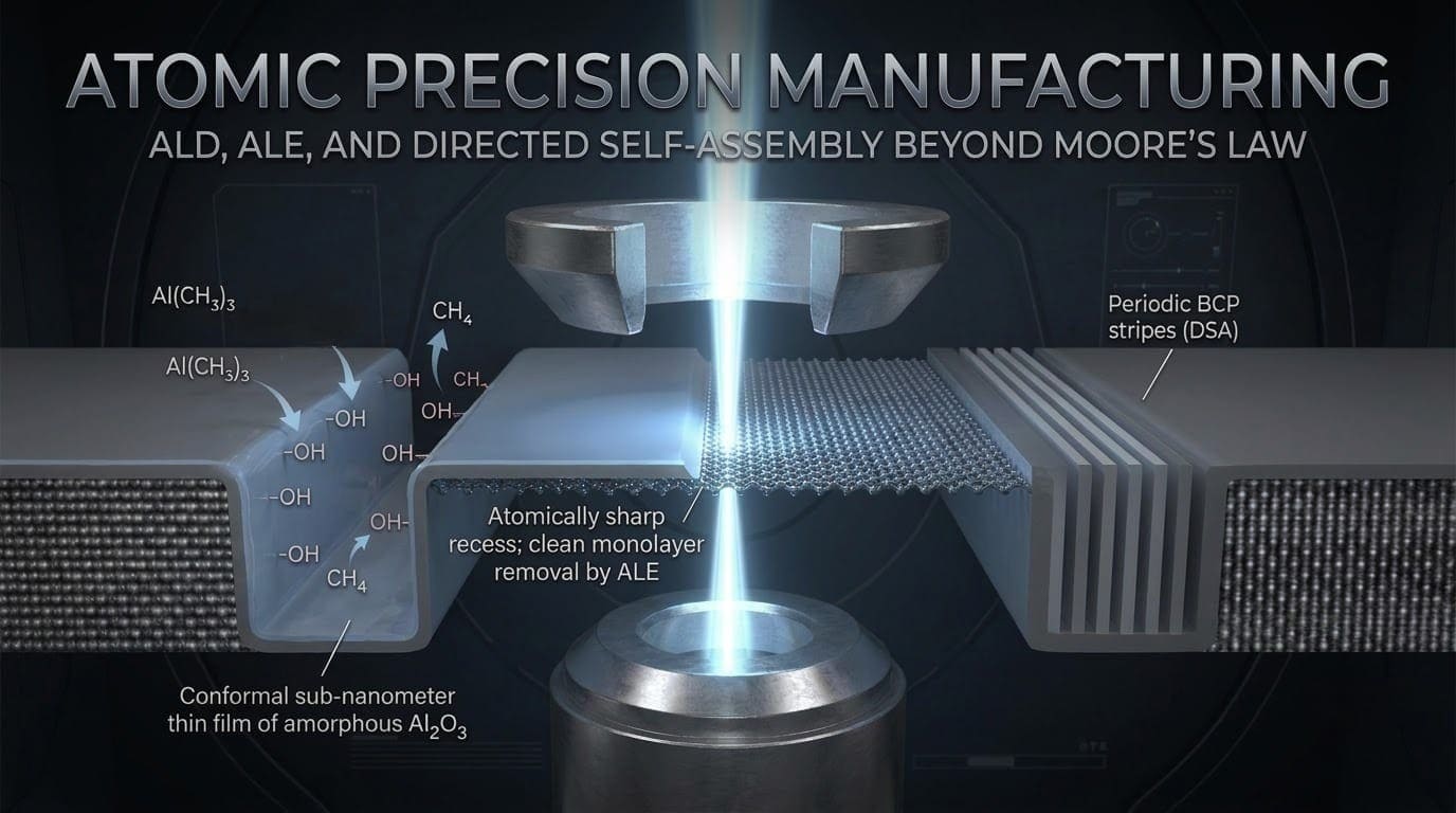
The deposition of aluminum oxide (Al₂O₃) illustrates this self-saturating surface chemistry through a four-stage binary cycle:
- Precursor Exposure (TMA Pulse): Trimethylaluminum [Al(CH₃)₃] vapor reacts with accessible surface hydroxyl groups (–OH), forming surface-bound –Al(CH₃)₂ species and releasing volatile methane (CH₄).
- Inert Gas Purge: High-purity nitrogen or argon purges unreacted TMA molecules and methane byproducts from the reaction chamber.
- Co-reactant Exposure (Water Pulse): Water vapor (H₂O) doses the chamber, hydrolyzing the remaining methyl ligands, producing additional methane, and regenerating surface hydroxyl groups.
- Secondary Purge: The chamber is evacuated or purged, leaving a newly chemisorbed sub-nanometer-scale layer ready for the subsequent cycle.
The process is self-limiting because the reaction depends on the availability of appropriate surface sites. Once the accessible sites have reacted, additional precursor cannot continue depositing material indefinitely under the same conditions. Steric effects also contribute to this behaviour because surface bound precursor fragments occupy physical space and restrict access to neighbouring sites. The resulting growth per cycle depends on the precursor chemistry, surface termination, temperature, exposure conditions and transport into the structure, so an ALD cycle should not be interpreted as automatically corresponding to one complete atomic layer.
This surface-reaction mechanism provides atomic layer deposition with an unmatched capability for conformality over complex three-dimensional geometries. Unlike physical vapor deposition or standard chemical vapor deposition, which are constrained by line-of-sight arrival and precursor gas-phase diffusion gradients, the self-saturating surface kinetics of ALD ensure near-unity step coverage across high-aspect-ratio trenches. In contemporary semiconductor manufacturing, this characteristic is essential for depositing sub-nanometer gate dielectrics, metallic work-function layers, and diffusion barriers inside gate-all-around nanosheet architectures and high-density 3D NAND memory arrays. Typical growth-per-cycle values of approximately 0.1 nanometers provide absolute thickness control while maintaining stoichiometric integrity across the entire wafer surface.
ALD therefore demonstrates a central principle of atomic precision manufacturing. Precise control does not necessarily require physically positioning individual atoms. By controlling the chemistry of a surface, the manufacturing process can determine when and where additional material is able to form.
Atomic Layer Etching (ALE): Directional and Isotropic Subtractive Precision
Manufacturing also requires subtraction. Structures must be etched, recessed and separated, and conventional plasma or ion based etching can become increasingly difficult to control as dimensions shrink. Unwanted physical sputtering, surface damage, roughness and changes in feature profiles can become significant when only a few nanometres of material need to be removed.
Atomic layer etching, or ALE, approaches this problem by separating surface modification from material removal. In a representative silicon process, the surface can first be chemically modified through chlorination. The modified surface is then exposed to energetic ions under conditions selected to remove the chemically altered layer while minimizing uncontrolled sputtering of the underlying material.
Atomic layer etching achieves atomic subtraction by decoupling surface reaction into two primary modes:
- Directional (Plasma-Assisted) ALE: Utilizes chemical halogenation (e.g., surface chlorination forming a volatile reaction layer) followed by low-energy ion bombardment calibrated strictly below the physical sputtering threshold of silicon to remove anisotropic features without subsurface lattice damage.
- Isotropic (Thermal) ALE: Operates via sequential fluorination and coordinated ligand-exchange reactions to remove conformal material evenly from 3D structures, maintaining etch rates reliably down to fractions of an angstrom per cycle without ion-induced shadowing defects.
ALE is therefore conceptually complementary to ALD. ALD provides a mechanism for highly controlled material addition, while ALE provides a mechanism for highly controlled material removal. Together, they provide two fundamental operations required for manufacturing at extremely small dimensions.
Spatial Patterning: High-NA EUV Lithography and Directed Self-Assembly
Controlling the amount of material is only part of the manufacturing problem. The material must also be placed in precisely defined locations. Lithography provides this spatial control, and advances in semiconductor manufacturing have pushed lithographic systems toward increasingly demanding resolution and pattern fidelity requirements.
Electron beam lithography can directly write nanoscale patterns using a focused electron beam and remains an important tool for research and prototyping. However, because features are written sequentially, throughput becomes a major limitation for large scale manufacturing. Extreme ultraviolet lithography addresses this problem through optical projection using radiation with a wavelength of approximately 13.5 nanometres.
While extreme ultraviolet lithography at a 13.5-nanometer wavelength enables resolution beyond deep ultraviolet limits, feature scaling exposes severe stochastic printing limits. Because resist sensitivity requires lower exposure doses to maintain manufacturing throughput, the finite number of photons absorbed per unit volume induces pronounced photon shot noise. This stochastic variability, compounded by secondary electron scattering within chemically amplified or metal-oxide resists, directly causes line-edge roughness, line-width roughness, and nano-bridging defectivity. Consequently, implementing high-numerical-aperture EUV optical projection requires co-optimizing photoresist chemistry and surface priming to ensure that the higher spatial frequencies captured by the 0.55 numerical aperture system successfully transfer into functional wafer patterns without catastrophic yield loss.
High numerical aperture EUV systems are being developed to improve imaging resolution further. Increasing numerical aperture allows finer spatial information to be projected, but it does not eliminate the underlying stochastic nature of photon absorption and resist chemistry. At advanced dimensions, manufacturing precision therefore depends not only on the optical resolution of the exposure system but also on how reliably the entire resist process converts that exposure into the intended structure.
Nanoimprint lithography provides a different strategy. Instead of optically projecting each feature, a nanoscale template physically replicates a pattern into a resist. This parallel approach illustrates another important principle of nanomanufacturing: high precision must ultimately be combined with sufficient throughput and reproducibility to become technologically useful.
When Matter Builds Its Own Structure
Not every nanoscale feature needs to be directly written. In some materials, molecular interactions can cause structures to organize spontaneously. This phenomenon, known as self-assembly, provides a bottom up route to nanoscale manufacturing.
Block copolymers are a particularly important example. They contain chemically different polymer blocks that are connected to one another, preventing complete macroscopic phase separation while still allowing the two blocks to segregate over nanometre length scales. Depending on composition and processing conditions, the polymers can form ordered morphologies such as lamellae, cylinders or spheres.
The thermodynamics of this process can be described using the Flory Huggins interaction parameter, χ, which represents the energetic incompatibility between the polymer segments. The product χN, where N represents the degree of polymerization, helps determine whether the system remains disordered or undergoes microphase separation. Increasing χ can permit ordered structures to form at smaller characteristic dimensions, making high χ block copolymers particularly attractive for nanoscale patterning.
However, spontaneous self-assembly does not automatically provide the positional accuracy required by a technological device. Directed self-assembly addresses this limitation by using chemical or topographical patterns on a substrate to guide the organization of the polymer domains. A larger scale pattern can therefore determine where the nanoscale domains form, while the molecular system generates the smaller features through its own thermodynamic organization.
This creates a useful connection between top down and bottom up manufacturing. Instead of using lithography to directly write every nanoscale feature, the lithographic pattern can provide guidance while molecular interactions generate the finer structure. Similar principles are being investigated for organizing nanoparticles, nanowires and other nanoscale building blocks using chemical interactions and external fields.
Sub-Angstrom Metrology: Aberration-Corrected STEM and Electron Spectroscopy
Fabricating an atomic scale structure is only part of the challenge. Researchers must also determine whether the structure actually matches the intended design. At these dimensions, characterization becomes a form of metrology, because small differences in composition, atomic arrangement or interface structure can produce large changes in material behaviour.
Aberration corrected scanning transmission electron microscopy has become one of the most powerful approaches for investigating materials at atomic resolution. In STEM, a focused electron probe is scanned across the specimen while scattered electrons are collected by detectors. High angle annular dark field imaging is particularly valuable because its signal is strongly dependent on atomic number under appropriate experimental conditions, producing the characteristic Z contrast used to distinguish atomic columns with different compositions.
Aberration correction allows the electron probe to be focused to sub angstrom dimensions under suitable conditions, making individual atomic columns resolvable in crystalline materials. The technique does not simply provide a smaller image. It allows researchers to investigate how atoms are arranged within interfaces, defects, doped regions and nanoscale structures.
The information can be extended through spectroscopy. Electron energy loss spectroscopy can provide information about elemental composition, bonding and electronic structure, allowing researchers to investigate not only where atoms are located but also how their chemical and electronic environments differ.
At the same time, atomic resolution does not mean that interpretation is automatic. Specimen thickness, electron channeling, multiple scattering, crystal orientation, detector geometry and beam induced damage can influence the measured signal. Atomic scale metrology therefore requires careful experimental design and complementary characterization rather than simply acquiring a high resolution image.
In Situ Metrology and Machine Learning for Closed-Loop Nanomanufacturing
The increasing capabilities of fabrication and characterization are beginning to change how these processes can be connected. Traditionally, manufacturing was performed first and characterization followed. A structure was produced, measured and then evaluated. At atomic dimensions, a more integrated approach is becoming increasingly attractive.
In situ microscopy can allow researchers to observe structural changes while materials are being deposited, transformed or exposed to controlled environments. Instead of examining only the final state, researchers can investigate nucleation, growth, diffusion, phase transformations and defect formation as they occur. This information can reveal why a particular manufacturing process produces a desired structure or why it deviates from the target.
Computational methods can add another layer to this process. Automated image analysis can identify atomic columns and defects, while machine learning can assist in extracting patterns from large microscopy datasets. In principle, measurements obtained during fabrication could be used to adjust process parameters and improve the subsequent manufacturing step.
This points toward a closed loop approach to nanomanufacturing in which fabrication, characterization and process control operate as parts of a connected system. The objective would not simply be to automate manufacturing, but to create processes capable of detecting deviations at increasingly small length scales and responding before those deviations propagate into larger defects.
Pillars of the Atomic-Scale Manufacturing System
- Atomic Layer Deposition (ALD): Self-limiting additive chemisorption providing step coverage over high-aspect-ratio 3D architectures.
- Atomic Layer Etching (ALE): Self-terminating subtractive removal that eliminates plasma damage and preserves crystalline stoichiometry.
- High-NA EUV & DSA: Complementary spatial patterning balancing optical throughput with molecular-level thermodynamic resolution.
- Aberration-Corrected STEM & EELS: Sub-angstrom analytical metrology validating chemical states and atomic column placement via Z-contrast imaging.
The Industrial Test of Atomic Precision
The most difficult challenge may not be demonstrating atomic precision in a laboratory. It is maintaining that precision across large areas, enormous numbers of devices and commercially relevant production timescales.
An experimental process may produce an exceptionally well controlled structure over a small region, but industrial manufacturing must also achieve high throughput, low defect density, uniformity, reproducibility, process stability and acceptable cost. A technique that provides extraordinary resolution but cannot operate reliably over large areas will therefore have limited manufacturing value.
This is why atomic precision manufacturing is becoming an ecosystem rather than a single technology. Lithography provides spatial information, self-assembly can generate nanoscale order, ALD can add material with controlled surface chemistry, ALE can remove material through self-limiting reactions, and atomic scale characterization can determine whether the resulting structure matches the intended design.
The convergence of these technologies represents a broader change in nanotechnology. Manufacturing is moving beyond the simple fabrication of increasingly small shapes toward the controlled engineering of matter itself. At nanometre dimensions, interfaces, defects, surface chemistry and atomic arrangements can determine whether a material behaves as intended.
The ultimate goal is not necessarily to position every atom individually. It is to understand the chemical and physical rules that govern matter at these dimensions and use those rules to make fabrication increasingly predictable.
Atomic precision manufacturing represents an essential paradigm shift from purely scaling down physical dimensions to engineering the fundamental thermodynamics that govern material formation. As atomic layer deposition, atomic layer etching, advanced lithography, molecular self-assembly, and sub-angstrom electron metrology converge, the traditional boundary between materials science and fabrication engineering dissolves. Industrial scaling below the 1-nanometer node will ultimately depend on building closed-loop, data-driven manufacturing platforms capable of regulating surface chemical states in real time.
The central question facing advanced microelectronics is determining which technological path will dominate sub-1nm patterning: continuing to scale high-numerical-aperture EUV lithography through multivariable optical and resist corrections, or adopting hybrid directed self-assembly schemes where molecular thermodynamics dictate pitch resolution.
We welcome your insights, experiences, and technical perspectives on this critical manufacturing transition in the comment section below.
Scientific references:
- Barah, O. O., David, M. & Joseph, M. Atomic-scale characterization: A review of advances in microscopy, spectroscopy, and machine learning. Journal of Materials Science: Composites 6, 6 (2025). https://doi.org/10.1186/s42252-025-00073-x
- Chai, Z., Childress, A. & Busnaina, A. A. Directed assembly of nanomaterials for making nanoscale devices and structures: Mechanisms and applications. ACS Nano 16, 17641–17686 (2022). https://doi.org/10.1021/acsnano.2c07910
- Cooper, K. Scalable nanomanufacturing: A review. Materials 10, 1379 (2017). https://doi.org/10.3390/ma10121379
- Jeong, S. J., Kim, J. Y., Kim, B. H., Moon, H. S. & Kim, S. O. Directed self-assembly of block copolymers for next generation nanolithography. Materials Today 16, 468–476 (2013). https://doi.org/10.1016/j.mattod.2013.11.002
- Kanarik, K. J., Lill, T., Hudson, E. A., Sinha, A., Aghazadeh, F., Tan, S. & Marks, J. Atomic layer etching: Rethinking the art of etch. The Journal of Physical Chemistry Letters 9, 4814–4821 (2018). https://doi.org/10.1021/acs.jpclett.8b00997
- Kessels, W. M. M., Devi, A., Park, J. S., Ritala, M., Yanguas-Gil, A. & Wiemer, C. Atomic layer deposition. Nature Reviews Methods Primers 5, 66 (2025). https://doi.org/10.1038/s43586-025-00435-6
- Krivanek, O. L., Lovejoy, T. C., Dellby, N., et al. Aberration-corrected STEM for atomic-resolution imaging and analysis. Journal of Microscopy 259, 165–172 (2015). https://doi.org/10.1111/jmi.12254
- Liddle, J. A. & Gallatin, G. M. Nanomanufacturing: A perspective. ACS Nano 10, 2995–3014 (2016). https://doi.org/10.1021/acsnano.5b03299
- Mathew, P. T., Rodriguez, B. J. & Fang, F. Atomic and close-to-atomic scale manufacturing: A review on atomic layer removal methods using atomic force microscopy. Nanomanufacturing and Metrology 3, 167–186 (2020). https://doi.org/10.1007/s41871-020-00067-2
- Puurunen, R. L. Surface chemistry of atomic layer deposition: A case study for the trimethylaluminum/water process. Journal of Applied Physics 97, 121301 (2005). https://doi.org/10.1063/1.1940727
- 11. Zhang, J., Li, Y., Cao, K., et al. Advances in atomic layer deposition. Nanomanufacturing and Metrology 5, 191–208 (2022). https://doi.org/10.1007/s41871-022-00136-8